PCB Inspection and Metrology
PCB Inspection and Metrology
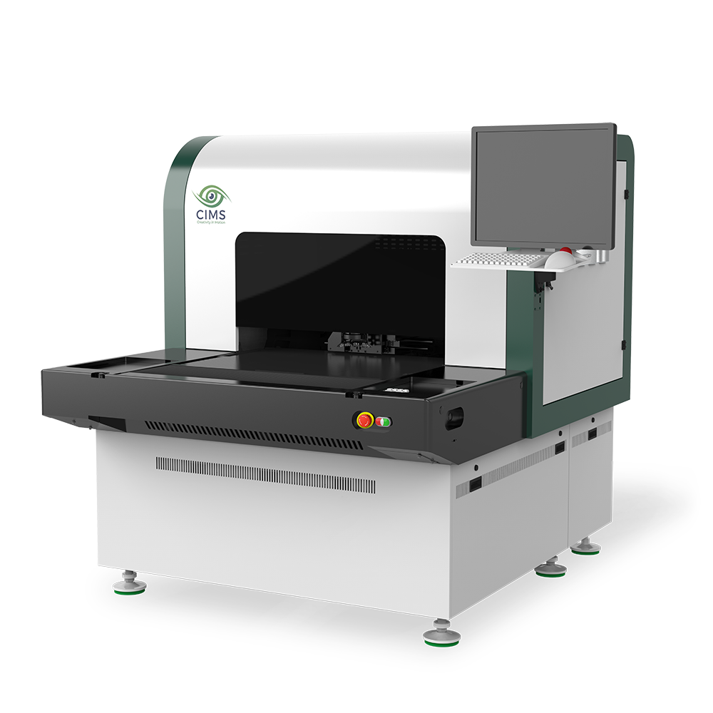
CIMS AOI and AVI systems combined with 2D and 3D metrology tools are capable to scan lines of down to 4 µm and are widely used in all segments of PCB industry.

Automated Optical Inspection Systems (AOI)
Automated optical inspection (AOI) is a crucial step for PCB manufacturers, during which inner and outer layers are carefully inspected to assure functionality and reliability resulting in high yield production.
CIMS offers wide range of AOI systems for all segments of PCB industry – from IC Substrates and HDI, flex and rigid flex to mainstream multi-layer boards. CIMS AOIs are helping our customers to dramatically increase yield of PCB manufacturing process as well as improve quality of the final product.
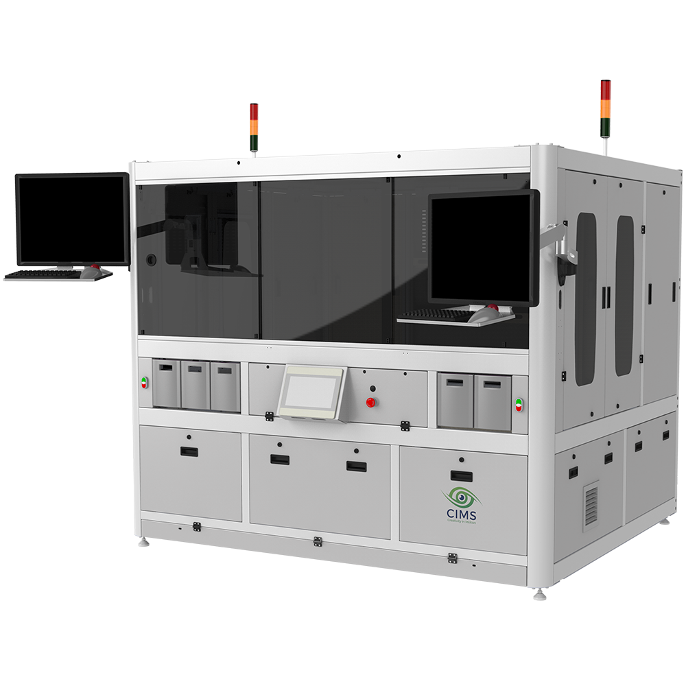
Automated Final/Visual Inspection Systems (AFI/AVI)
Automated visual/final inspection (AVI/AFI) is a process performed at the final stages of IC Substrate manufacturing ensuring defects-free product. The dense structure of IC Substrates requires optical inspection at high resolutions and capable of detecting wide variety of surface defects.
CIMS AVI solutions are designed to meet specific quality requirements of IC Substrates manufacturers. Final inspection with CIMS technology provides optimal detection capabilities coupled with minimal false calls and performed at high throughput.


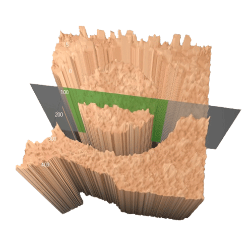
Metrology and add-on inspection options
CIMS add-on options are designed to further enhance inspection capabilities of AOI and AVI systems. Those options can be integrated with CIMS equipment offering a new layer of quality assurance for our customers.
CIMS add-on options include unique 2D and 3D metrology capabilities that can be integrated with AOI systems and allowing to perform advanced measurements during the normal inspection cycle. Other options enable integrating defects data collection, classification and reporting capabilities into verification stage of inspection process.