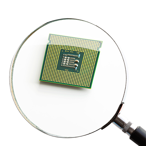
Semiconductors Inspection and Metrology
Semiconductors Inspection and Metrology
CIMS inspection capabilities are applied to advanced packaging, Wafer-level and panel-level-packages (including fan-out and fan-in applications) which are further enhanced with 2D and 3D metrology options integrated within the inspection tool.

Inspection of Semiconductor devices
The inspection of Semiconductor devices is a crucial step in Microelectronics production process. It involves highly accurate inspection for defects and multiple production stages, recording and outputting the results and generating QA related information that can be accessed and acted upon immediately in order to improve the overall yield.
CIMS offers automated inspecton solutions for patterned wafers as well as various fan-out and fan-in products for both WLP (wafer-leve-packaging) and PLP (panel-level-packaging). CIMS AOIs for Microelectronics are helping our customers to dramatically increase yield of their manufacturing process as well as improve quality of the final product.
Metrology and add-on inspection options
CIMS add-on metrology options are designed to further enhance inspection capabilities of Semiconductor devices. Those options can be integrated with CIMS equipment offering a new layer of quality assurance for our customers.
CIMS add-on options include unique 2D and 3D metrology capabilities allow to perform advanced measurements during the normal inspection cycle. This eliminates the need for an offline dedicated metrology systems and shortens QA feedback cycle.
