CIMS Press Release
AI Revolution Reshaping the Future of PCB Manufacturing
Article by Val Kaplan, vice president of marketing
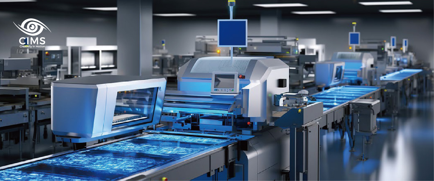
In the rapidly evolving landscape of PCB manufacturing, the integration of machine learning (ML) in the context of smart factories is ushering in a new era of efficiency, adaptability, and competitiveness within the industry. This article explores how ML is revolutionizing various facets of smart factories, including predictive maintenance, quality control, production, and inventory optimization. By harnessing the power of data-driven insights and automation, ML is enabling factories to proactively address issues, optimize processes, and enhance product quality. This transformative technology not only minimizes downtime but also paves the way for agile, cost-effective, and sustainable manufacturing operations. The article sheds light on real-world applications, challenges, and the promising future of ML in the Smart factory ecosystem.

Val Kaplan
What are Smart Factories?
A Smart factory is typically defined as an advanced manufacturing facility that utilizes cutting-edge technologies, automation, and data-driven processes to optimize its operations, improve efficiency, enhance productivity, and enable more agile and flexible production.
In a Smart factory, various components, including machines, equipment, and systems, are interconnected and communicate with each other, as well as with a central control system, through connectivity solutions such as the Internet of Things (IoT) and other methods. This interconnectedness allows for real-time data collection, analysis, and decision making, leading to proactive maintenance, rapid adaptation to changing demands, and improved product quality.
Most advanced Smart factories are characterized by their ability to leverage artificial intelligence, machine learning, robotics, and other advanced technologies to streamline operations and drive innovation in manufacturing processes.
The integration of machine learning (ML) and artificial intelligence (AI) in Smart factories has the potential to transform traditional manufacturing processes into agile, data driven, and highly efficient operations. The se technologies enable factories to respond to changing demands, reduce costs, enhance product quality, and improve overall competitiveness in the global market.
In recent years, PCB factories have been gradually adapting various Smart factory concepts although this process has been relatively slow and limited to the most advanced and forward-looking companies. Also, Smart factories in the PCB industry tend to mainly focus on the equipment interconnectivity and process data gathering and consolidation while data analysis is still mainly done by human expert operators rather than AI.
On the other hand, the amount and dimensionality of data that can potentially be gathered from multiple PCB processes is simply too extensive for human brains to process. This is where machine learning and artificial intelligence hold the most promise and could outperform even the best human experts.
The following are the primary areas in which ML and AI technologies can provide the most significant benefits for Smart PCB factories.
Machine Learning for Predictive Maintenance
Once the information from multiple processes is continuously fed into a central data repository, AI models can analyze data from different sensors and equipment to predict when machinery might fail. For example, such models can be trained to detect inconsistencies or gradual subtle changes from sensor readings, as well as juxtapose these data with the data from downstream processes, to find patterns.
Such multi-dimensional analyses involving huge numbers of interrelated variables is a natural fit for AI technology while being an impossible task for humans, even with the help of the most advanced analytical (non-AI) software. Such tasks are particularly suitable for unsupervised AI, specifically through techniques like clustering and dimensionality reduction. These AI models are used for finding patterns in data without explicit labels or guidance.
In short, AI technology has the potential to deliver more effective proactive maintenance, reducing downtime and saving costs.
Machine Learning for Troubleshooting of Equipment and Processes
Machine Learning for Troubleshooting of Equipment and Processes Machine learning can be a valuable tool for troubleshooting and data-driven problem identification in PCB manufacturing. For example, ML algorithms, such as clustering or statistical models, are used to identify anomalies or outliers in the data. These anomalies can signal potential issues.
ML techniques can also be applied to determine the root causes of anomalies or problems. This may involve correlation analysis, causal inference, or rule-based systems. Such systems would identify which factors or variables are most strongly associated with the detected anomalies, and direct maintenance staff to the right equipment and even suggest a solution.
In order to enable such tracing capabilities, each panel must carry a unique identifier, typically a 2D code (data matrix code, or DMC, is the most common type). This code will then be scanned at every production stage enabling the system to trace it back to every process equipment it went through during production process.
Machine learning and AI technology is also being gradually adopted within AOI and AFI/AVI processes. The ultimate goal is to reduce human operators’ involvement in defects verification to the minimum, if not eliminate it altogether, thereby streamlining the AOI process by making it faster and less prone to human errors.
In this application, the AI image recognition model is trained on an extensive set of real defects aiming at teaching it how to tell them apart from false calls such as non-critical contamination or acceptable process variations. In general, deep learning neural network AI is the most suitable technology for image recognition in general and optical inspection in particular.
Despite the promising potential, implementing ML for the AOI verification cycle is not without significant technological and conceptual challenges. The seemingly simple question, “What is a defect?”, may not have the same answers between market segments, among different PCB manufacturers, or even individual jobs within the same company.
Furthermore, defect specifications frequently change and evolve over time as a result of new processes, changing end user requirements, and PCB makers’ other various considerations. This means that one AI model may not be sufficient to cover all scenarios, and such models must be retrained on a regular basis with new data that better reflects the current situation. For example, an AI system would be unable to accurately identify defects that it had never been trained on or effectively filter out a previously unknown type of false calls.
Another challenge is determining the best tradeoff between two competing metrics: the filter rate (the number of true false calls removed by AI) and escapes, also known as underkill or false negatives (real defects that were incorrectly classified and filtered out as false calls by the AI model). The higher the filter rate, the more defects will escape, and vice versa. The correct approach to resolving this problem is to take a purely economic approach, weighing the benefit of having less verification equipment and reduced manpower against the cost of lower yield due to higher escape rate.
Finally, there is a type of agency dilemma where there is a conflict of interest between the PCB manufacturer’s motivation to cut costs and the end user’s interest for high quality. It should come as no surprise that the end user may reject their suppliers’ cost-cutting efforts through the use of new technology if they have the potential to negatively impact product quality, which is their top priority. This is why they may be reluctant to accept any ML implementation by their suppliers that might jeopardize that goal.
Harnessing Machine Learning and AI for Smart Factories
PCB manufacturers, on the other hand, are in the business of making money, and cost savings with such technology directly translate to higher profit margins, though they may face resistance from their customers, particularly those with significant bargaining power.
Finally, there are practical and technicalchallenges associated with AI developmentand implementation, the most significantof which is the collection and processing ofmassive amounts of high-quality pre-classified(labeled) data required to develop a viablemodel. The data provided by PCB manufacturerscan be messy, particularly in terms of classification accuracy. As a result, AI developers would have to expend significant effort to clean and reclassify the data in order to make it suitable for AI model training purposes. This is a time-consuming process that frequently results in the discarding of some amounts of low-quality data.
In conclusion, the success or failure of AI technology adoption for the AOI process is primarily determined by the optimal balance between the rate of escapes and the overall filter rate, resolving issues around accurate defect specs while periodically retraining AI models with new and relevant data, and navigating the agency dilemma between PCB manufacturers and their customers.
Machine Learning for Optimizing Production Processes
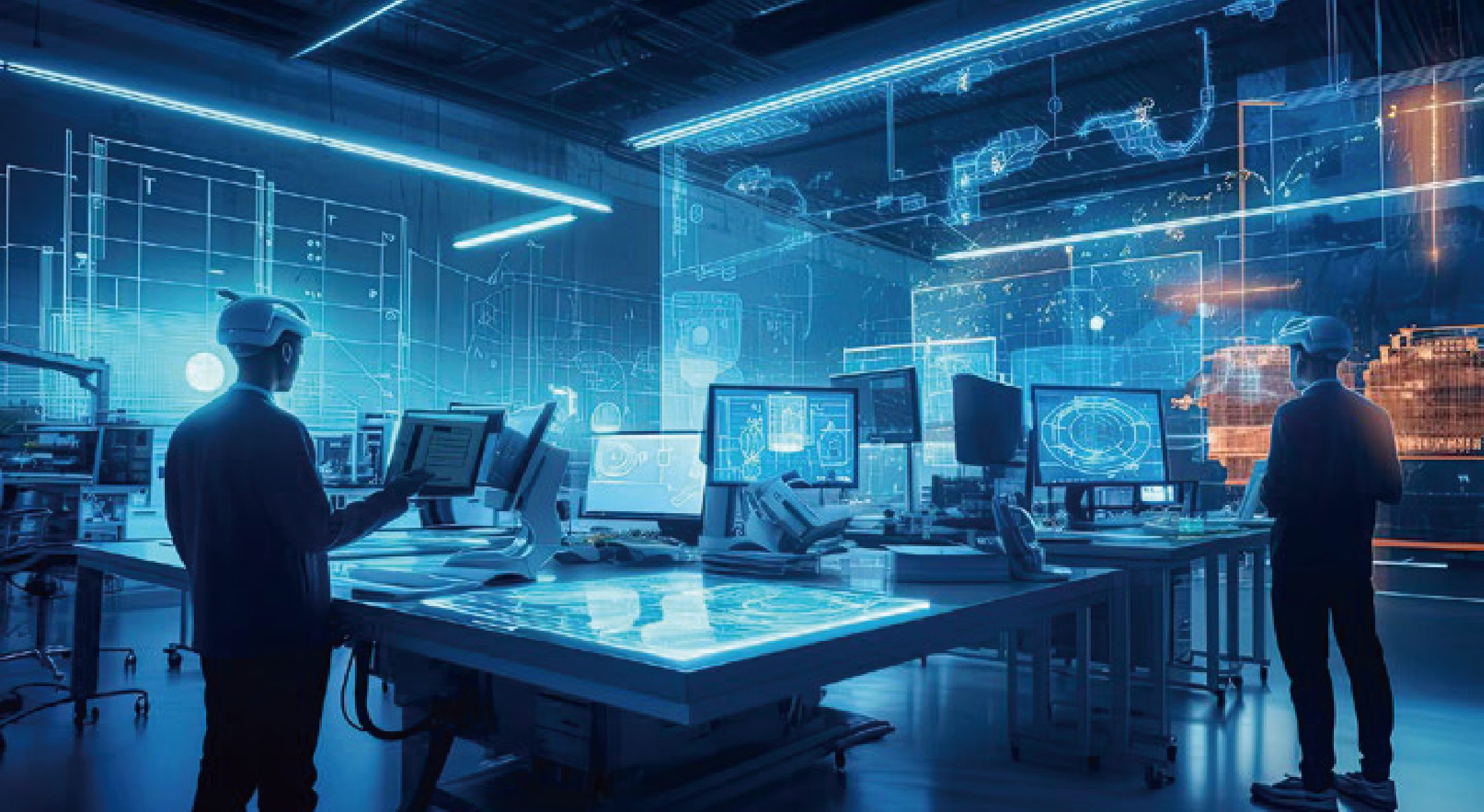
ML can significantly enhance the optimization of PCB production processes, including production planning and scheduling, as well as inventory management. For example, ML models can analyze historical sales data, market trends, and other relevant factors to forecast future demand more accurately. This information helps in setting production targets.
ML algorithms can optimize resource allocation by considering factors like machine availability, labor capacity, and job specifics (such as complexity and required process flow, as well as raw material availability) to create efficient production process routes and schedules.
For example, the AI models that we have developed allow users to identify the optimal route through production processes down to a specific equipment, which maximizes efficiency and yield while minimizing production time and the costs. Such a model learns from the vast database of historical data on the performance of each individual equipment with different types of jobs and their effect on the overall defect types and rates.

One of the biggest practical challenges in Smart factory adoption and implementation is the difficulty in collecting reliable and consistent data from processes and machinery.
There are two main reasons for it:
1. Lack of connectivity of some equipment, particularly the older machinery that makes data collection difficult if not impossible,
2. Lack of common data exchange protocols and formats within the PCB industry.
The lack of connectivity can sometimes be addressed by installing dedicated sensors that transmit the relevant data wirelessly. In other cases, a special software can be used to grab information directly from the user interface and send it to the central database by Ethernet or Bluetooth.
The lack of common formats and protocols basically means that data from different processes must first be converted into some type of common format in order to be useable and then “stitched” together along relevant features and data dimensions.
Also, some equipment manufacturers deliberately prevent external users from accessing and sharing their data, attempting to lock-in their customers within the ecosystem of that company’s products and solutions. In such cases, the connection can be refused, or data can be encrypted to prevent third parties from reading it.
We chose the opposite approach, ensuring safe and secure access to all data generated by our systems as well as data kept in our databases, using SDK (software development kit). This enables other users, such as third-party developers or customers’ IT engineers, to take full advantage of the wide range of actionable information available from AOI or AVI/AFI systems.
The Future of ML and AI Technologies in PCB Manufacturing
There is little doubt that, for better or worse, AI will transform almost every aspect of our lives; this process has already begun. Only a few years ago, technologies like ChatGPT were considered science fiction, yet they are now available to everyone. Every industry, including ours, has the potential to be transformed by ML and AI technologies.
What can we expect in the future once the above-mentioned challenges are resolved? One possibility is that AI systems may take over more of the day-to-day decision-making on how to manage PCB manufacturing operations, even down to optimizing each individual piece of equipment. When combined with material handling automation, such a system has the potential to automate PCB manufacturing to unprecedented levels.
Intelligent manufacturing solutions based on AI will be able to resolve quality issues on their own by automatically tweaking various parts of the process, reroute production flow to maximize yield, and optimize equipment and material usage, relying on human operators only in a few exceptional cases. Once AI can control and optimize all elements of PCB fabrication, from quoting and CAD to manufacturing and quality inspection, Smart factories
will truly become intelligent, ushering in a new era of innovation and technological progress.
Published by PCB007