Systems installed
Customers worldwide
Countries served
Our products
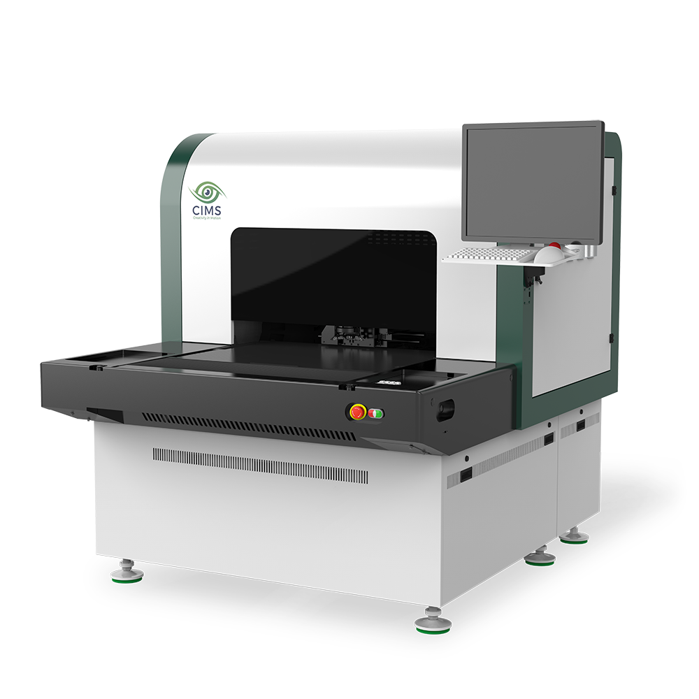
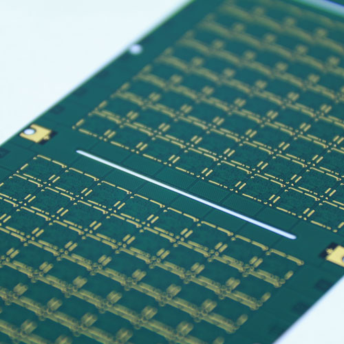
PCB Inspection and Metrology
CIMS AOI and AVI systems combined with 2D and 3D metrology tools are capable to scan lines of down to 4 µm and are widely used in all segments of PCB industry.
Semiconductors Inspection and Metrology
CIMS inspection capabilities are applied to advanced packaging, Wafer-level fan-out and fan-out panel-level-package while using 2D and 3D metrology tools integrated with the inspection tool.
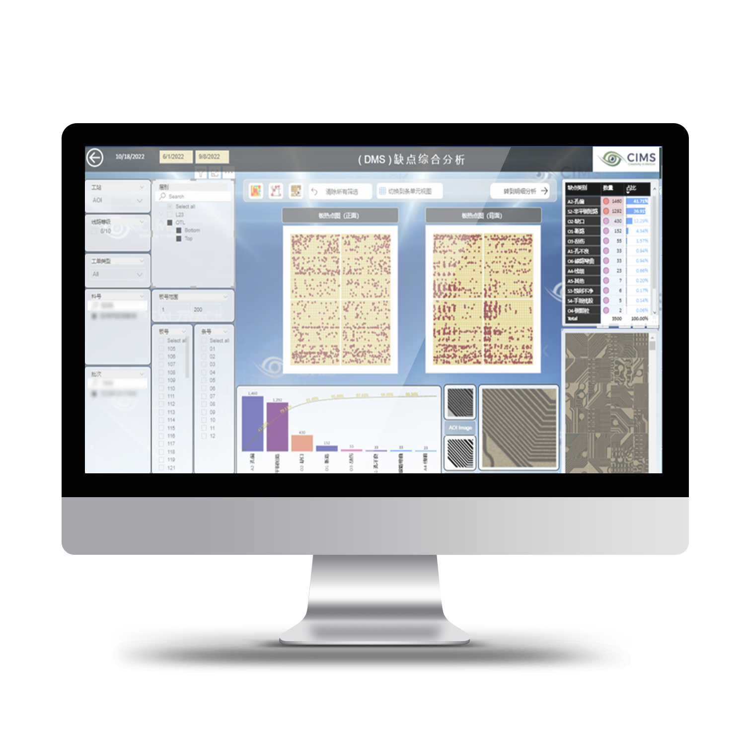
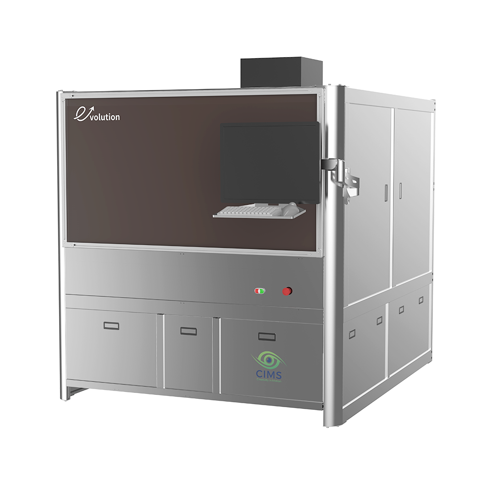
Digital Solutions for Smart Factory
CIMS software solutions for smart factories include various data automation options, data management and analysis software as well as AI-based verification and false calls reduction solutions.
Frontend Software for intelligent manufacturing
Advanced software solutions by Ucamco* for automated PCB pre-production and front-end workflow and high performance CAM software for all types of PCB makers and customized solutions for high-end equipment manufacturers.
*Ucamco is a fully owned company by CIMS
High accuracy photoplotters for PCB and FPD industries
Our wide range of extremely accurate Ucamco* laser photoplotters are available in various throughput and resolutions configurations to suit our customer’s photo tooling production needs and performance requirements.
*Ucamco is a fully owned company by CIMS
Material handling and smart factory automation
Smart factory automation and standalone automation equipment by Transystem* are designed to integrate with the most sophisticated PCB production environment, ranging from loaders/unloaders and AGVs to complete turn key automation solutions for smart factories.
*Transystem is a majority owned company by CIMS
Our markets
Solutions for Printed Circuit Boards (PCB) IC Substrates manufacturing
CIMS offers series of AOI and AVI solutions for manufacturers producing wide variety PCB types and designs including IC Substrates. Our advanced automated inspection and metrology solutions are widely used by virtually every top PCB producer in the world and are renowned for their reliability and superior performance.
CIMS provides dedicated inspection solutions for all major segments of PCB market: IC Substrates, HDI PCB, Flex PCB as well as conventional MLB PCB. Our integrated 2D and 3D metrology options add another layer of powerful functionality by further enhancing capabilities and scope of CIMS systems.
CIMS also offers multiple software solutions for PCB including Ucamco CAD/CAM design software, pre-CAM solutions and many others. In addition, CIMS Ucamco photoplotters cover imaging needs of all types of PCB fabricators.

Inspection and metrology solutions of Semiconductors
Fan-Out packaging is the enhancement of standard wafer-level packaging (WLP) where the connections are “fanned-out” of the chip surface, enabling more external I/Os. Fan-out WLP provides a smaller package footprint along with improved thermal and electrical performance compared to conventional packages, and allows having higher number of contacts without increasing the die size.
Panel level packaging (PLP) involves embedding both active (IC) and passive components directly within PCB during its fabrication structure as opposed to mounting components on the finished board.
CIMS solution provides a reliable and cost-effective inspection and metrology solution to ensure high quality of the fan-out WLP and PLP boosting yield and productivity offering the optimal trade-off between escapes and overkill.
LTCC – low temp co-fried ceramics
LTCC is a substrate technology that provides reliable, high density electrical interconnection for active and passive components on ceramics base. LTCC packages offer a number of advantages over traditional packaged circuits in terms good thermal conductivity combines with low coefficient of thermal expansion, robustness against mechanical and thermal stress and low prduction cost. LTCC technology is widely used in mobile communication technology.
CIMS offers dedicated solutions for inspection of wide variety of LTCC products at different production stages, various types of ceramics and range of substrate thicknesses. Thanks to our innovative metrology, verification and data management solutions, our solutions take LTCC inspection to the next level.


Imaging solutions for Flat Panel Displays (FPD)
CIMS Ucamco large format high resolution photoplotters are specifically designed to meet imaging needs of FPD manufacturers.
All models make use of the latest technology in linear and rotary encoders. In combination with the state-of-the-art optical-mechanical imaging unit using granite base, linear motor and air bearings it achieves the highest possible positioning and imaging accuracy.
CIMS Ucamco photoplotters an automatic film load- and unloading system as well as an online connection to the film processor. The film handling system is very simple, to maximize accuracy and reliability producing extremely high quality photo tools for Flat Panel Displays (FPD) as well as for Chemical Milling and other high-resolution graphic applications.
About CIMS

CIMS is a global leader in machine vision, imaging technologies smart factory and frontend software solutions that address the diverse inspection and metrology needs of PCB and Semiconductors industries.
CIMS advanced solutions are widely used by nearly all world leading electronics manufacturers, making CIMS products one of the essential tools within the global electronics manufacturing supply chain.
In the PCB market, CIMS provides automated optical inspection solutions (AOI), automated final/visual inspection solutions (AVI/AFI), metrology and add-on inspection options, smart factory integration and data management software as well as cutting edge AI-based verification solutions, dedicated to enhancing production processes and yield in Printed Circuit Board (PCB), IC Substrates, High Density Interconnect PCB (HDI PCB) and Flex and Rigid-flex PCB (FPC).
In the Semiconductors market, CIMS offers inspection solutions for wafer-level and panel-level packaging segments, particularly for fan-out and fan-in products, as well as various 2D and 3D metrology options for in-line quality control at various stages of packaging fabrication process.
CIMS also offers wide range of software solutions for PCB fabricators that include full CAM/CAD design packages (Ucam product family) as well as various Pre-CAM solutions and other software that is essential for PCB production.
CIMS also provides high resolution/high accuracy photoplotters by Ucamco for the imaging needs of PCB and FPD (Flat Panel Display) manufacturers which are widely used with those industries.
Worldwide service centers
